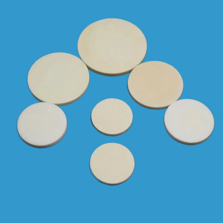
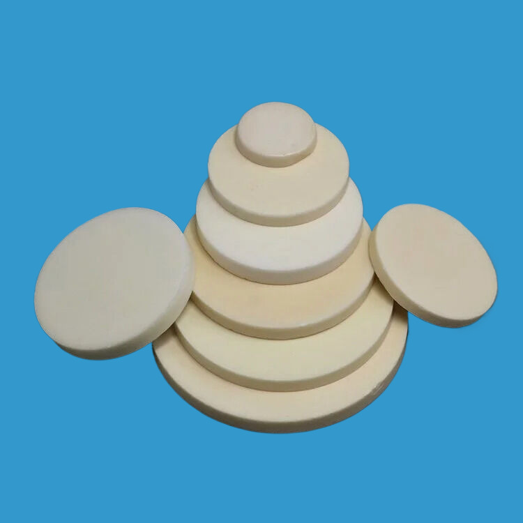
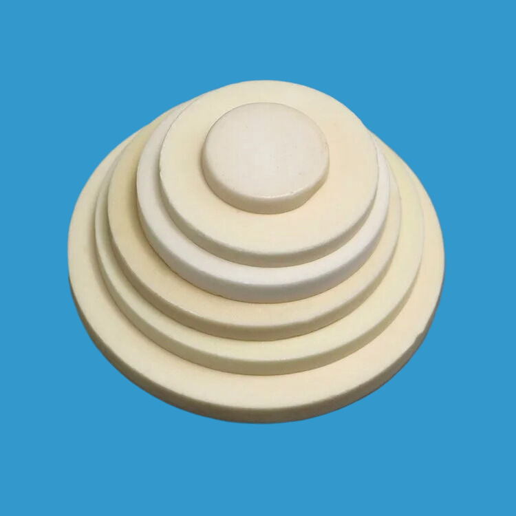
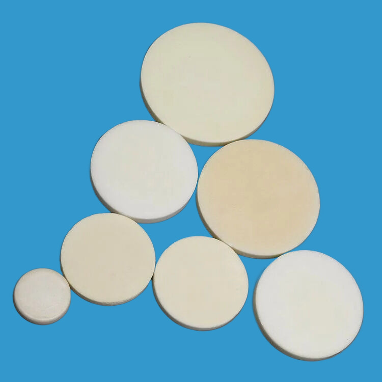
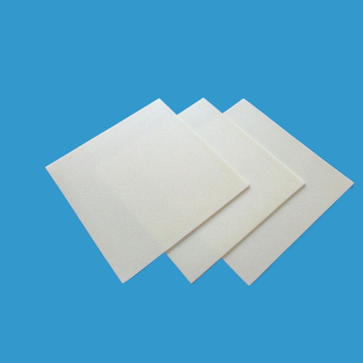
Semiconductor ceramic wafer plate alumina ceramic disk
Diameters can range from 1mm to 306mm
Thicknesses from 0.2mm to 20mm
Material:Alumina ceramic 95% 96% or 99%
Size:According to drawings or samples
Torlerance:+/- 0.02mm
Lead time:10-30 days
Delivery:Air Express (DHL/UPS/TNT/ FedEx)
Payment Term: PayPal; T/T; L/C etc.
Shipment: by sea by air by courier by post etc.
Semiconductor ceramic wafer plate is one of the important tools in semiconductor industry, which is widely used in wafer preparation, grinding, cleaning and other links in semiconductor production. It is usually a round disc with a diameter of 8 inches or 12 inches, a thickness of hundreds of microns to several millimeters, and a highly pure crystal structure.
Alumina ceramics purity: 95%, 96% 99%, 99.5% 99.7%
Ceramic wafer advantage:
1).Excellent electrical insulation
2).High hardness
3).Relatively low strength and fracture toughness
4).Resistance to wear and corrosive
5).Excellent thermal stability
6).Resistance to high temperatures
7).High electrical resistivity
8).Good chemical stability and resistance
9).High corrosion resistance
Alumina ceramics is one of the most widely used ceramic materials in the semiconductor industry, Semiconductor alumina ceramic wafer plate main characteristics include high hardness, high strength, wear resistance, corrosion resistance and so on. In addition, alumina ceramics have excellent insulation properties and thermal stability, which can withstand high temperature and pressure environments.
Semiconductor ceramic wafer plate is an important material in the semiconductor industry, used to manufacture various chips, such as microprocessors, memory, sensors and so on. The size of Semiconductor ceramic wafer plate is one of the key manufacturing parameters, which directly affects the performance and cost of the chip. The main dimensions of Semiconductor ceramic wafer plate include diameter and thickness, and tolerance is also an important parameter.
The diameter of Semiconductor ceramic wafer plates is usually 2 inches (50.8 mm), 3 inches (76.2 mm), 4 inches (101.6 mm), 5 inches (127 mm), 6 inches (152.4 mm), 8 inches (203.2 mm), etc. Among them, the 4-inch Semiconductor ceramic wafer plate is the most commonly used. Semiconductor ceramic wafer plates with different diameters have different characteristics and advantages and disadvantages in terms of production, process, equipment, cost and so on.
The thickness of Semiconductor ceramic wafer plate is usually 525 microns, 625 microns, 725 microns, etc. The thickness of the Semiconductor ceramic wafer plate is also affected by tolerances. Tolerance is the allowable error set in the process of manufacturing Semiconductor ceramic wafer plate to ensure the accuracy of the size. The size of the tolerance directly affects the cost and manufacturing difficulty of Semiconductor ceramic wafer plate.
Material | Alumina ceramic 95% 96% or 99% Alumina Ceramic |
Size | According to drawings or samples |
Torlerance | +/- 0.02mm |
Lead time | 10-30 days |
Delivery | Air Express (DHL/UPS/TNT/ FedEx) |
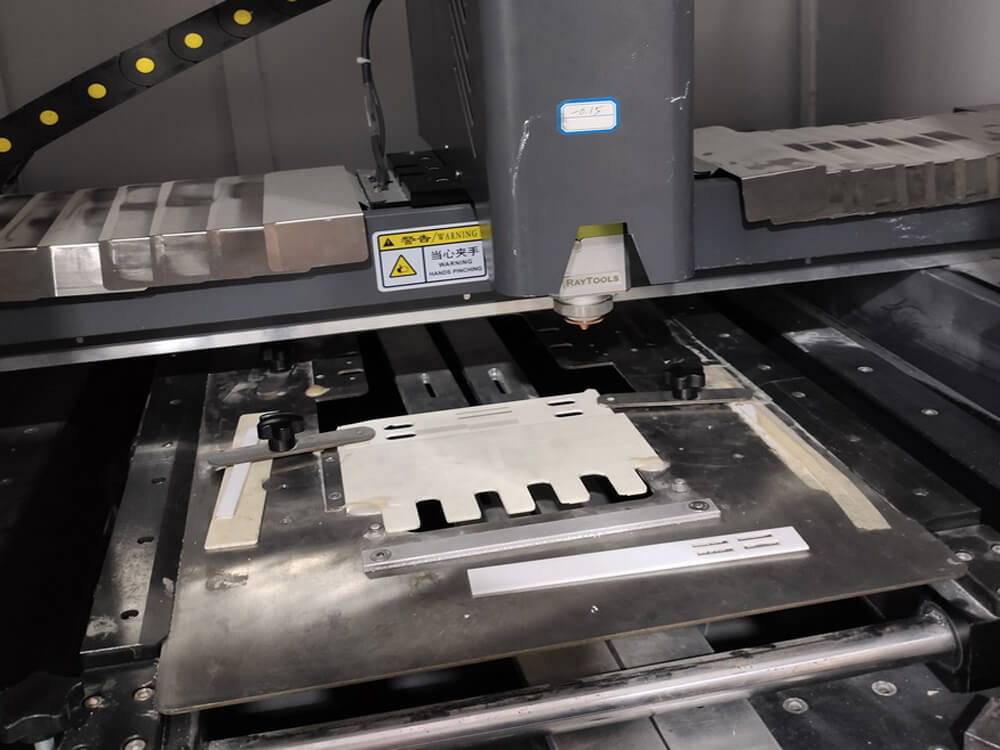
Precision machining ceramic video
Machining parameters of ceramic parts
The following are some of our ceramic parts processing parameters. For specific precision ceramic parts processing parameters and processing flow, please contact us.
- Dimensional accuracy: up to 0.001mm
- Surface finish: Up to Ra0 · 03
- Concentricity: up to 0.003mm
- Parallelism: up to 0.002mm
- Inner hole tolerance: minimum machined 0.005mm
- Straight groove: The narrowest machined groove is 0.1x100mm
- Cylindricity: up to 0.004mm
- Linear tolerance: up to 0.001mm
Our Services - Need any help!
Find the latest ceramic parts quotes, accurate ceramic parts parameters, comprehensive ceramic parameter performance? Please contact us.
Our ceramic parts engineers communicate directly with customers, quickly understand the parameters, customer requirements details, efficient and fast to give solutions and reply information, provide quick consulting quotes.
- Support sample manufacturing and testing
- Support drawing
- Multiple ways of communication
- Support customization
- Engineer direct communication
- On-time and fast shipment
Contact Form
Tips:If you have any questions, please contact us, we will get back to you within 1 hour.
